Exam 2 Makeup Lab
You can ask your TA to test and grade your code during your lab section in lab 11, or your lab section in the next week (April 15-17). The latter one is the deadline for the makeup.
You can choose to do this lab to make up for 15% of EXAM 2 (7.5 of 50 points). The lab also helps you understand more details of the control design for the multi-cycle implementation.
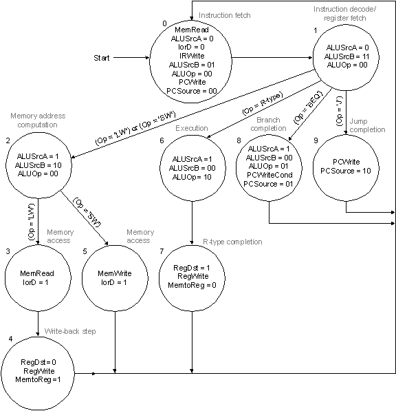
You are going to use verilog to program (1) the 10-state control as shown in the following figure, and (2) the revised 20-state control as specified in the explanation of question 8, exam 2.
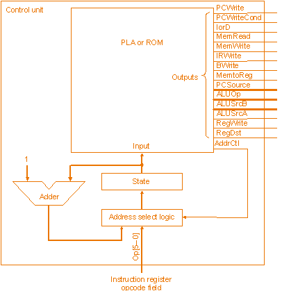
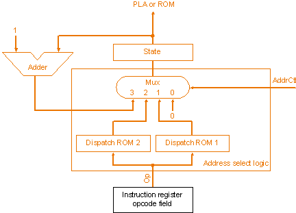
Your implementation should be based on the "microprogram-counter + dispatch ROMs" approach. The left figure gives an overview of such an implementation, and the right figure details the “address select logic”.
 |
 |
Use MaxPlus MegaWizard Plug-in Manager to generate a ROM with 4-bit address input and 7-bit output. Do not use registered input or output. The format of the 7-bit output is
MemRead(1):MemWrite(1):RegWrite(1):ALUOp(2):AddrCtl(2)
For simplicity, we are generating four control signals of five bits rather than all control signals of sixteen bits. AddrCtl is for sequencing control. Then, determine the related truth table and translate it into the .mif file associated with the ROM. For example:
DEPTH = 16;	% Memory depth and width are required %
WIDTH = 7;	% Enter a decimal number %

ADDRESS_RADIX = DEC;	% Address and value radixes are optional %
DATA_RADIX = BIN;	% Enter BIN, DEC, HEX, or OCT; unless %
			% otherwise specified, radixes = HEX %
CONTENT
    BEGIN
    [0..15]     : 0000000;	% default value %
    0		: 1000011;	% state 0: MemRead asserted, ALUop=00, AddrCtl=11
    1		: 0000001;	% ALUop = 00, AddrCtl = 01 (for dispatch 1)
    ... 			% fill other rows here %
    END
STEP 2: Generate module DISPATCH1_ROM (opcode, state) and DISPATCH2_ROM (opcode, state)
Use MaxPlus MegaWizard Plug-in Manager to generate the two dispatch ROMs
for state 1 and state 2, respectively. Each ROM has 6-bit address input for the
op-code and 4-bit output for the state. Determine the truth
tables and then write the asscoiated .MIF files.
Elaboration: PLA or a collection of gates is more efficient for these two parts. We use ROM for simplicity.
STEP 3: Write module CONTROL (opcode, memread, memwrite, regwrite, aluop, state, clk)
You will program for the adder, state register, mux, and connect them to three ROMs your have created. Use memread, memwrite, regwrite, and aluop as registered outputs. In other words, their values change on clock edges. For example:
wire[6:0] rom_out;
always @ (posedge clk) begin
	memread = rom_out[6];
	...
end
The state output is used for testing.
STEP 4: Test your implementation using for the following op-codes:
            R-type	000000
            LW		100011
            SW		101011
            BEQ		000100
            JUMP	000010
For each op-code you should see the correct state transition. See the testing output.
STEP 5: Make the following changes to your programs (keep a copy of your original files):
-
Change your state register in your CONTROL module to 5-bit
-
Use MaxPlus MegaWizard Plug-in Manager to change your CONTROL_ROM so that it has 5-bit address input.
-
Edit the associated .mif file. First change the memory depth to 32, then edit the ROM content for the new FSM. See the table in Question 8 Explanation.
You may finish this step within 10 minutes. Test your new control using the following testing cases: